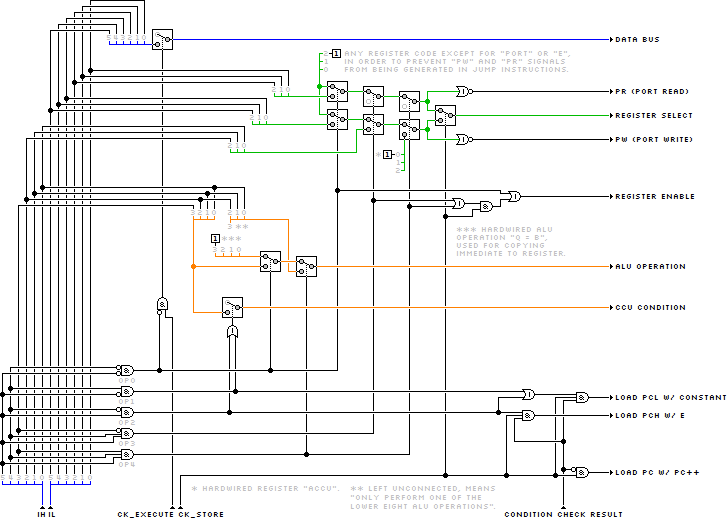
flags bus and joining them into a new 4 bits wide bus.

| Main website: | https://mosfetkiller.de/?s=warp-1 |
| Documentation: | https://mosfetkiller.de/warp-1/doc |
| Name | Properties | Description |
| Data bus | 6 bits | Numbers from 0 to +63 (unsigned) or -32 to +31 (signed) |
| Address bus | 12 bits | Up to 4096 words of program memory addressable |
| Internal memory | 7x 6 bits | Accumulator, flags register and 5 general purpose registers A..E
|
| Flags | C,O,N,Z,S,H | Carry, Overflow, Negative, Zero (ALU), Stack (switches port mode from I/O to stack), Halt (halts CPU) |
| Program memory | EEPROM | Should really be replaced by a punch card reader |
| Stack memory | 24x 6 bits | 24 words of LIFO memory in external I/O/Stack Unit |
| Ports | 1x 6 bits I/O | Used to communicate with I/O/Stack Unit |
| User interface | 1x 6 bits I/O | Data written to the port in I/O mode is currently being output on LEDs, data read from the port is currently read from a set of switches accessible to the user on the I/O/Stack Unit |
| Clock speed | max. ??? Hz | Two-phased clock, thus half an instruction per cycle |
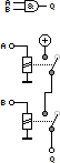
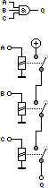
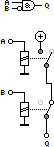
| — (blue) | 6 bit parallel data bus |
| — (orange) | 4 bit parallel data bus |
| — (green) | 3 bit parallel data bus |
| — (black) | 1 bit data line |
| — (purple) | 8 bit parallel data bus |
| Example: |
Extracting four flags C,O,N,Z from the 6 bits wide flags bus and joining them into a new 4 bits wide bus. |
|
ACCU and 5 general purpose registers A, B,
C, D, E are freely available to the programmer to store
any 6-bit value.ACCU is always the first operand of any
ALU operation. The E register is always the HIGH address for
(conditional) far jumps.r2 r1 r0 | Register |
0 0 1 | ACCU |
0 1 1 | A |
0 1 0 | B |
1 1 1 | C |
1 1 0 | D |
1 0 0 | E |
FLAGS register, which is freely accessible to the programmer.
The flags register is being updated after every ALU operation, except for when the flags register is selected as
destination register. In that case, the flags coming straight out of the ALU are being discarded.| Flag | Bit in register | Description |
C | 0 | Carry flag. The carry flag is being set, if an addition produces a result too large to be stored in a 6 bits wide register. It is also a low active borrow in "subtract with carry" operations. |
O | 1 | Overflow flag. (Useful in signed operation mode only.) Compares both input and output Zero flags (ALU). If they differ, an overflow (change in sign) occured and this flag is being set. |
N | 2 | Negative flag. (Useful in signed operation mode only.) If the result of an ALU operation is positive, this flag is being set. (Bit 5 of result is just being copied into this flag.) |
Z | 3 | Zero flag. This flag is being set if the result of an ALU operation equals zero or if two operands being compared are exactly equal. |
S | 4 | Stack flag. (Only useful in combination with the optional, external I/O/Stack unit.) If cleared, the port is in I/O mode. If set, the port is in Stack mode. |
H | 5 | Halt flag. If set, the CPU clock halts immediately until the user resets the machine. |
FLAGS register
is being referred to by an individual 3-bit number:r2 r1 r0 | Register |
1 0 1 | FLAGS |
PORT is accessible to the programmer. It behaves like a regular register; data can be written
to and read from it. The port's main use is to connect it to an external I/O/Stack unit.
In combination with this module, the port works in two different modes, determined by the status of the
Stack flag.PORT
is being referred to by an individual 3-bit number:r2 r1 r0 | Register |
0 0 0 | PORT |
PC) holds the address of the instruction to decode next.
The PC is 12 bits wide, thus consists of two 6 bits wide registers PCH (upper 6 bits) and
PCL (lower 6 bits). These registers are not accessible to the programmer in
ALU and "Copy Immediate to Register" operations, but they can be modified by performing
jump operations. See 2.1.2d (Conditional) Short jump and
2.1.2e (Conditional) Far jump for more information.i to destination register d
(see 2.1.1 Registers for register codes).| Bit | 11 10 9 8 7 6 5 4 3 2 1 0 |
1 1 0 d2 d1 d0 i5 i4 i3 i2 i1 i0 |
o on Accumulator as first operand and source register s as second operand.
The result is being stored in destination register d
(see 2.1.1 Registers for register codes).B.| Bit | 11 10 9 8 7 6 5 4 3 2 1 0 |
0 0 o3 o2 o1 o0 d2 d1 d0 s2 s1 s0 |
o3 o2 o1 o0 | Operation | Flags affected | |
0 0 0 0 | Q = A + B | Add without carry | C O N Z |
0 0 0 1 | Q = A + B + C | Add with carry | C O N Z |
0 0 1 0 | Q = A - B = A + /B + 1 | Subtract without carry | C O N Z |
0 0 1 1 | Q = A - B + C = A + /B + C | Subtract with carry | C O N Z |
0 1 0 0 | Q = A & B | Logic AND | - - - Z |
0 1 0 1 | Q = A | B | Logic OR | - - - Z |
0 1 1 0 | CMP A, B (A - B) | Compare (subtract w/o saving result) | C O N Z |
0 1 1 1 | TEST A, B (A & B) | Test (logic AND w/o saving result) | - - - Z |
1 0 0 0 | Q = B | No operation | - - - - |
1 0 0 1 | Q = /B | One's complement | - - - - |
1 0 1 0 | Q = B - A = B + /A + 1 | Subtract without carry | C O N Z |
1 0 1 1 | Q = B - A + C = B + /A + C | Subtract with carry | C O N Z |
1 1 0 0 | Q = B >> 1 | Shift right | C - - - |
1 1 0 1 | Q = B << 1 | Shift left | C - - - |
1 1 1 0 | Q = A ^ B | Logic XOR | - - - Z |
1 1 1 1 | Q = A & /B | Logic AND, one operand inverted | - - - Z |
o on Accumulator as first operand and immediate value i as second operand.
The result is being stored in the Accumulator.B.| Bit | 11 10 9 8 7 6 5 4 3 2 1 0 |
1 1 1 o2 o1 o0 i5 i4 i3 i2 i1 i0 |
o3 o2 o1 o0 | Operation | Flags affected | |
0 0 0 0 | Q = A + B | Add without carry | C O N Z |
0 0 0 1 | Q = A + B + C | Add with carry | C O N Z |
0 0 1 0 | Q = A - B = A + /B + 1 | Subtract without carry | C O N Z |
0 0 1 1 | Q = A - B + C = A + /B + C | Subtract with carry | C O N Z |
0 1 0 0 | Q = A & B | Logic AND | - - - Z |
0 1 0 1 | Q = A | B | Logic OR | - - - Z |
0 1 1 0 | CMP A, B (A - B) | Compare (subtract w/o saving result) | C O N Z |
0 1 1 1 | TEST A, B (A & B) | Test (logic AND w/o saving result) | - - - Z |
c. If the condition check is TRUE, PCL
(see 2.1.1d Program counter for more information) is being loaded with immediate
value i. If the condition check is FALSE, normal program execution continues.| Bit | 11 10 9 8 7 6 5 4 3 2 1 0 |
0 1 c3 c2 c1 c0 i5 i4 i3 i2 i1 i0 |
c3 c2 c1 c0 | Flags | Mnemonic | Arithmetic comparison/test | Logical test | ||
0 0 0 0 | don't care | JMP | - | - | - | |
0 0 0 1 | Z | JE,JZ | A == B | A equals B | Result == 0 Result equals zero | |
0 0 1 0 | !Z | JNE,JNZ | A !== B | A unequals B | Result !== 0 Result unequals zero | |
0 0 1 1 | O & !Z | JL | A < B | A is less than B | - | |
0 1 0 0 | O | Z | JLE | A <= B | A equals or is less than B | - | |
0 1 0 1 | !O & !Z | JG | A > B | A is greater than B | - | |
0 1 1 0 | !O | Z | JGE | A >= B | A equals or is greater than B | - | |
0 1 1 1 | C | JC | - | C | Carry flag is set | |
1 0 0 0 | !C | JNC | - | !C | Carry flag is not set | |
1 0 0 1 | !N & !Z | JP | Result > 0 | Result is positive | - | |
1 0 1 0 | !N | Z | JZP | Result >= 0 | Result equals or is greater than zero | - | |
1 0 1 1 | N & !Z | JN | Result < 0 | Result is negative | - | |
1 1 0 0 | N | Z | JZN | Result <= 0 | Result equals or is less than zero | - | |
1 1 0 1 | - | - | - | - | - | |
1 1 1 0 | - | - | - | - | - | |
1 1 1 1 | - | - | - | - | - |
c. If the condition check is TRUE, PCL
is being loaded with immediate value i and the value of register E is being copied to PCH
(see 2.1.1d Program counter for more information).
If the condition check is FALSE, normal program execution continues.| Bit | 11 10 9 8 7 6 5 4 3 2 1 0 |
1 0 c3 c2 c1 c0 i5 i4 i3 i2 i1 i0 |
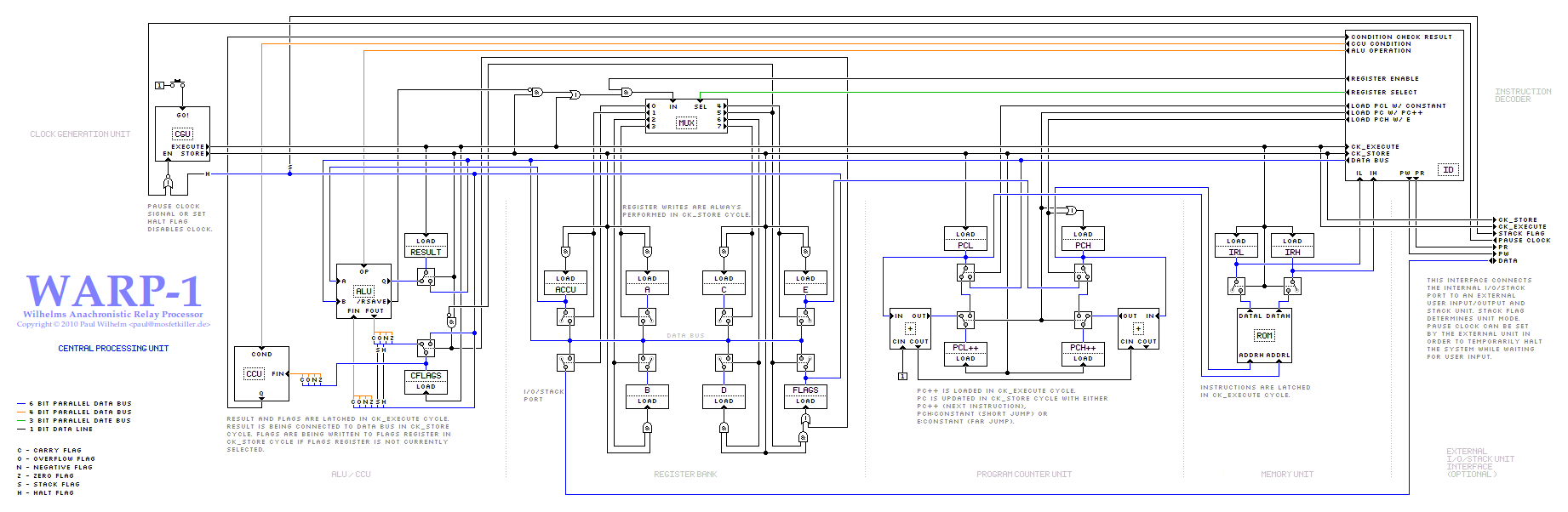
 The basic logic gates NOT, XOR, OR and AND are used to generate control signals throughout the CPU and I/O/Stack Unit.
| NOT | OR | XOR | AND | |||||
 |
 |
 |
 |
 |
 |
 |
 |
 |
| (Inverter) | (two inputs) | (three inputs) | (two inputs, output inverted) |
(two inputs) | (two inputs, output non-buffered) |
(two inputs) | (three inputs) | (two inputs, one inverted) |
 Bus switches are used for selective interconnection of buses. Since these modules only consist
consist of relays (analog components) they are bidirectional. Each bus switch has three
sets of data lines (A,B,C) and one select input, which when LOW connects A to B and when HIGH connects A to C.
Either of data line sets A or B may be left unconnected.
Bus switches are used for selective interconnection of buses. Since these modules only consist
consist of relays (analog components) they are bidirectional. Each bus switch has three
sets of data lines (A,B,C) and one select input, which when LOW connects A to B and when HIGH connects A to C.
Either of data line sets A or B may be left unconnected.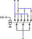
 Registers are used for storing and reading 6 bits of data simultaneously. The bits in one register
can be interpreted as a number between 0 and +63 (unsigned) or -32 and +31 (signed).
These modules are actually transparent latches, but in the context of this project we refer to them as registers.
The logical levels of data lines
Registers are used for storing and reading 6 bits of data simultaneously. The bits in one register
can be interpreted as a number between 0 and +63 (unsigned) or -32 and +31 (signed).
These modules are actually transparent latches, but in the context of this project we refer to them as registers.
The logical levels of data lines 0..5 are latched on the rising edge of LOAD and can then
be read back during LOAD low state.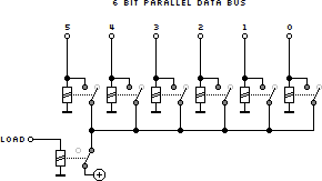
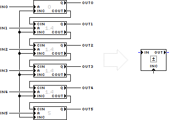
 Two half-adders are used for incrementing the program counter (
PCL and PCH).
These modules each have one input bus IN and one output bus OUT, each 6 bits wide.
Since there is only a carry input CIN used as second addend, only 0 or 1 can be added to the input.
Several of these modules can be cascaded using the carry output COUT.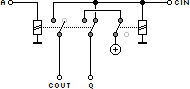
CIN input and
COUT output lines. The entirety of A and B lines is the input bus
IN and OUT respectively.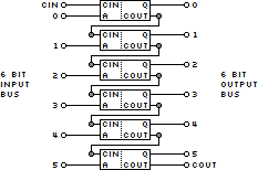
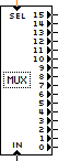 Multiplexers (mux) have a set of data inputs, one data output and a select input bus. The selected input signal
is being forwarded to the data output. Since these modules are designed using only relays
(analog components) every multiplexer is also a demultiplexer (demux) which forwards one data input signal to one of
several data outputs. The number of possible selectable data inputs/outputs depends on the number of select
input lines (2^n).
Multiplexers (mux) have a set of data inputs, one data output and a select input bus. The selected input signal
is being forwarded to the data output. Since these modules are designed using only relays
(analog components) every multiplexer is also a demultiplexer (demux) which forwards one data input signal to one of
several data outputs. The number of possible selectable data inputs/outputs depends on the number of select
input lines (2^n).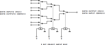
 The Condition Check Unit (CCU) is used by the Instruction Decoder (ID) in case of a conditional jump.
The module has two input busses
The Condition Check Unit (CCU) is used by the Instruction Decoder (ID) in case of a conditional jump.
The module has two input busses FIN and COND which take four flags (C,O,N,Z)
and a condition code respectively. Result output Q goes HIGH if the condition is complied with.
 The Arithmetic Logic Unit (ALU) performs simple arithmetic (ripple carry) and logic operations on one (
B)
or two (A and B) 6 bits wide operand values, thus generating a 6 bits wide output value Q.
The desired operation mode depends on the value of the 4 bits wide OP bus. A set of 4 input flags FIN
affects the operation and a set of output flags FOUT is being generated. The active low signal
/RSAVE tells the CPU whether the result Q shall be saved or discarded (this will be the case
whenever a CMP or TEST operation is being performed.)CTRL have to be set correctly for the individual operation to be performed.
Operands are A and B, result is Q.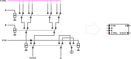
CIN and COUT lines, thus creating a 6 bits
wide ALU core.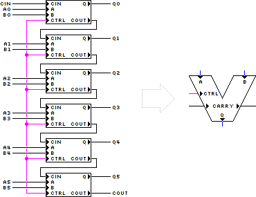
OP into the control signals CTRL mentioned above.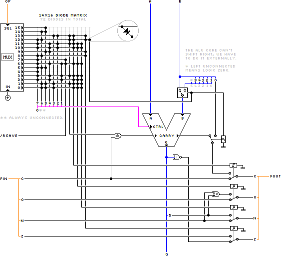
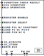 The instruction decoder controls all modules inside the CPU. A twelve bits wide instruction
word (
The instruction decoder controls all modules inside the CPU. A twelve bits wide instruction
word (IH and IL) is being decoded and a set of control signals is being generated,
depending on the instruction word itself, current clock cycle and the condition check result.5..0 of the instruction word represent a 6-bits wide immediate value, which is being
connected to the data bus in CK_EXECUTE cycle in all jump and ALU operations
except for ALU operation on Accu w/ Register (which does not require
an immediate value).PR (Port Read) signal is HIGH during one full instruction cycle
whenever any ALU operation with PORT
selected as source register is selected. Otherwise, PR is LOW.PW (Port Write) signal is HIGH during one full instruction cycle
whenever any ALU operation with PORT
selected as destination register is selected. Otherwise, PW is LOW.REGISTER SELECT
bus and the REGISTER ENABLE line, depending on current instruction and clock phase.| Instruction | Clock phase | REGISTER SELECT | REGISTER ENABLE | Description |
| Copy Immediate to Register | CK_EXECUTE | don't care * | LOW | (No register selected) |
| Copy Immediate to Register | CK_STORE | Instruction word bits [8..6] | HIGH | Destination register |
| ALU operation on Accu w/ Register | CK_EXECUTE | Instruction word bits [2..0] | HIGH | Source register |
| ALU operation on Accu w/ Register | CK_STORE | Instruction word bits [5..3] | HIGH | Destination register |
| ALU operation on Accu w/ Immediate | CK_EXECUTE | don't care * | LOW | (No register selected) |
| ALU operation on Accu w/ Immediate | CK_STORE | Hardwired ACCU register: 0b001 | HIGH | Destination is ACCU |
| (Conditional) Short jump | CK_EXECUTE | don't care * | LOW | (No register selected) |
| (Conditional) Short jump | CK_STORE | don't care * | LOW | (No register selected) |
| (Conditional) Far jump | CK_EXECUTE | don't care * | LOW | (No register selected) |
| (Conditional) Far jump | CK_STORE | don't care * | LOW | (No register selected) |
REGISTER SELECT value does not matter because REGISTER ENABLE is LOW.
Nevertheless, using the schematic below, REGISTER SELECT
does have a definite value of 0b100.ALU OPERATION
and CCU CONDITION buses, depending on current instruction.| Instruction | ALU OPERATION | CCU CONDITION | Description |
| Copy Immediate to Register | Hardwired ALU op. Q=B: 0b1000 | don't care * | Pass unchanged immediate through ALU |
| ALU operation on Accu w/ Register | Instruction word bits [9..6] | don't care * | One of all 16 ALU operations |
| ALU operation on Accu w/ Immediate | Instruction word bits [8..6] | don't care * | Only one of the lower 8 ALU operations |
| (Conditional) Short jump | don't care ** | Instruction word bits [9..6] | Conditional jump |
| (Conditional) Far jump | don't care ** | Instruction word bits [9..6] | Conditional jump |
CCU CONDITION value does not matter because the state of CONDITION CHECK RESULT
signal does not influence the execution of the current instruction. Nevertheless, CCU CONDITION
does have a definite value, namely the value of instruction word bits
9..6.ALU OPERATION value does not matter because during jump instructions
REGISTER ENABLE is always LOW, meaning that ALU result is not being stored in any register.
Nevertheless, ALU OPERATION does have a definite value
of 0b1000 (ALU operation Q=B).LOAD PCL W/ CONSTANT, LOAD PCH W/ E
and LOAD PC W/ PC++, depending on the type of current jump instruction and status of
CONDITION CHECK RESULT line during CK_STORE cycle.
During CK_EXECUTE cycle or if the current instruction does not imply any
conditional jump, all three lines are LOW.| Jump type | CONDITION CHECK RESULT | LOAD PCL W/ CONSTANT | LOAD PCH W/ E | LOAD PC W/ PC++ |
| SHORT | FALSE | FALSE | FALSE | TRUE |
| SHORT | TRUE | TRUE | FALSE | FALSE |
| FAR | FALSE | FALSE | FALSE | TRUE |
| FAR | TRUE | TRUE | TRUE | FALSE |
 The ROM is a non-volatile memory unit with one data bus and one address bus, both 12 bits wide.
This allows a maximum of 4096 words to be addressed. For reasons of simplicity and compactness,
integrated EEPROM circuits are being used in the current version of WARP-1.
Additionally, level shifters are neccessary in order to connect the
EEPROMs' low-voltage inputs/outputs to the rest of the system.
The ROM is a non-volatile memory unit with one data bus and one address bus, both 12 bits wide.
This allows a maximum of 4096 words to be addressed. For reasons of simplicity and compactness,
integrated EEPROM circuits are being used in the current version of WARP-1.
Additionally, level shifters are neccessary in order to connect the
EEPROMs' low-voltage inputs/outputs to the rest of the system.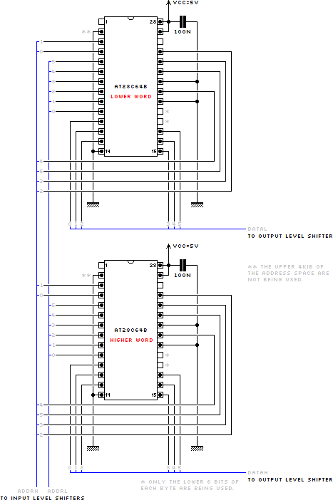
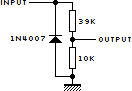
| INPUT |
An input level shifter is a two-resistor voltage divider which limits a high input voltage (+24V)
to a CMOS/TLL voltage level (+5V). The resistor connected to ground also pulls down the level shifter's
output, thus creating a logic LOW level when no input signal is present. Because relay coils are
connected directly to the input bus, free-wheeling diodes are neccessary in order to protect the
ICs input circuitry. |
 |
|
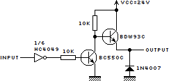
| OUTPUT |
An output level shifter consists of an emitter follower (BDW93C) in combination with an additional driver transistor (BC550C)
which, when turned on by a CMOS/TTL-compatible input signal, will connect the level shifter's output line to +24V,
thus transforming any CMOS/TTL signal into an open-emitter (relays do not have emitters, of course) signal able
to drive further relay's coils. Since the additional driver transistor inverts the input signal, the CMOS/TTL signal
is first being inverted by an HC4049 inverter. Because relay coils are connected directly to the output bus, free-wheeling
diodes are neccessary in order to protect the transistors. |
 |
 The CGU generates both
 CK_EXECUTE and CK_STORE signals. See 2.3 Timing
for more information on clock timing. Four cascaded non-retriggerable monoflops trigger each other
in a circular manner. A startup circuit initiates the oscillation by generating a very short pulse and
feeding it to the input of the first stage when the button "GO!" is being pressed. Pressing the button again
after that will have no effect. The first stage generates the CK_EXECUTE signal, the second
stage generates a pause (1), the third stage generates the CK_STORE signal and the fourth stage generates
another pause (2), then triggers the first stage again. The switches A and B at each stage can be used to
adjust the duration time of each stage, thus optimizing the overall clock signals and pause periods for speed.
When the enable input EN is low, the clock is being halted on the first stage (CK_EXECUTE) until
EN goes HIGH again.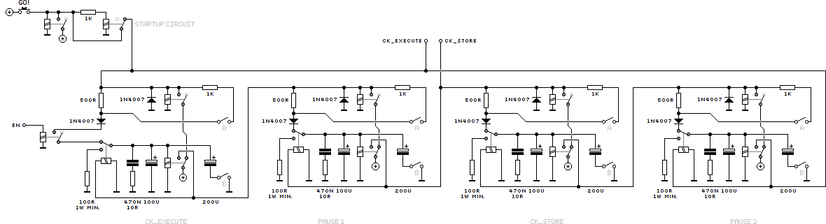
CK_EXECUTE and CK_STORE.
Both signals are being generated by the Clock Generation Unit (CGU). After both signals have been
emitted, one instruction cycle is complete.CK_EXECUTE.Q = B" is being selected, which means that the
ALU's input passes right through to its output. The result and flags are being latched to temporary registers
immediately in this cycle.PCH++ and PCL++ are being loaded with the value of the
program counter incremented by one.CK_STORE.FLAGS register, the ALU's output flags stored in another
temporary register are being loaded into the FLAGS register.PCL is being loaded with the immediate address value which has passed from the instruction
word through the ALU into the temporary result register in CK_EXECUTE
cycle and is now present on the data bus.E is being copied to PCH immediately if the CCU result is TRUE.PCH++ and PCL++ mentioned above.FLAGS register and Clock Generation Unit (CGU).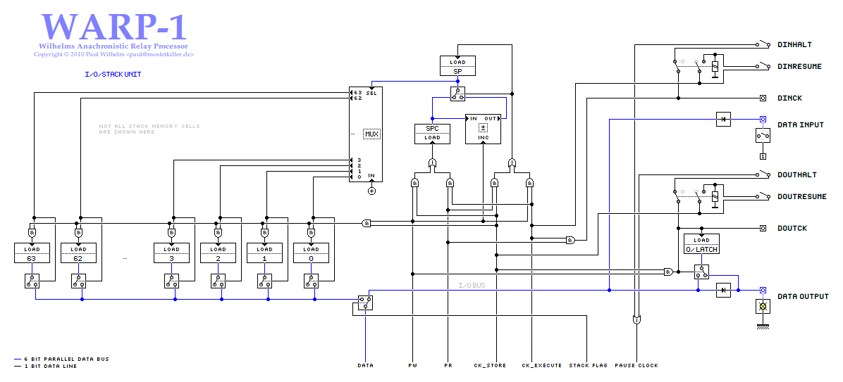
CK_STORE cycle of the instruction cycle
(which is most certainly too short for a human to accurately read the result), the data is being latched until
another "write to port" operation occurs (O/LATCH register). Additionally, a "data out" clock pulse
DOUTCK is being generated which can be useful when connecting a printer to the I/O port.DOUTHALT
must be closed. This way, the user can take his time reading the data and must then press the switch
DOUTRESUME in order to resume normal CPU operation.CK_EXECUTE cycle.
The data to be read into the CPU (in binary format) can be set by the user using six switches.CK_EXECUTE cycle,
the CPU can be halted automatically everytime user input is required. This way, the user can take his time
to respond to the request. To do so, the switch DINHALT must be closed.
In order to resume normal CPU operation, the switch DINRESUME must be pressed after
setting the correct data on the input switches.DINCK is
being generated everytime user input is required.SP to be incremented by one during
CK_EXECUTE cycle, thus selecting the next stack cell.
The data is being written to the currently selected stack cell during
CK_STORE cycle.SP exceeds a value of 63 (dec), an overflow occurs and SP
is set to it's minimum value, 0 (dec).CK_EXECUTE cycle.
The currently selected stack cell's value is being fed to the port for the CPU to read in and process
during CK_EXECUTE cycle. During CK_STORE
cycle SP is being decremented by one, thus selecting the previous stack cell.SP is being decremented below 0 (dec), an underflow occurs and SP
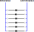
is set to it's maximum value, 63 (dec). This small module consists of six diodes with their anodes connected to an anodes bus
and cathodes connected to a cathods bus. This module is used to keep HIGH levels on a bus
from flowing into another part of the circuit.
This small module consists of six diodes with their anodes connected to an anodes bus
and cathodes connected to a cathods bus. This module is used to keep HIGH levels on a bus
from flowing into another part of the circuit.
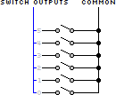
 This small module consists of six switches, each connected to a
 SWITCH OUTPUTS bus with one end.
The switches' other end is connected to a common terminal. This module can be used by the user to manually
set a specific binary value and feed it to the DATA INPUT bus.
 This small module consists of six lamps (which can be replaced by LEDs and corresponding resistors),
each connected to a
This small module consists of six lamps (which can be replaced by LEDs and corresponding resistors),
each connected to a LAMP INPUTS bus with one end. The lamps' other end is connected to
a common terminal. This module can be used to display binary values on the
DATA OUTPUT bus to the user.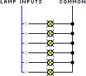
 This module takes any 6-bit value
 IN and increments it by one if the INC input is HIGH,
or decrements it by one if the INC input is LOW. The output value is present at OUT output.
The unit uses ripple carry, thus it takes a minimal amount of time for the unit to generate valid output.IN value.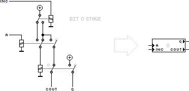
IN value.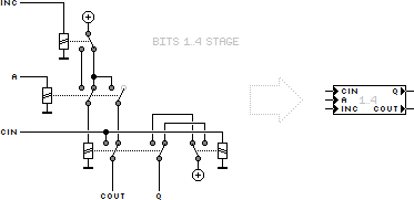
IN value.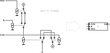
CIN and COUT lines.